http://flipchips.com/tutorial/assembly/nailing-ics-together/
存储芯片_百度百科
baike.baidu.com/view/6546463.htm
Translate this page
存储芯片是嵌入式系统芯片的概念在存储行业的具体应用。因此,无论是系统芯片系统芯片- 维基百科,自由的百科全书
https://zh.wikipedia.org/zh/系统芯片
Translate this page
系统芯片更强的功能要求它具备外部存储芯片,例如有的系统芯片配备了闪存。系统微机原理与接口技术习题与解析 - Page 114 - Google Books Result
https://books.google.com.hk/books?isbn=7302123810 - Translate this page
对 8088 系统对 8086 系统 4KB 2K )勺 2K>8 4KB 苛地址存储体偶地址存储体目 ... 举一反三:根据要求的存储空间容量和可供选用的存储器芯片的存储容量,计算所需 ...SoC - MBA智库百科
wiki.mbalib.com/wiki/SoC
Translate this page
SoC(System on Chip; 系统级芯片; 片上系统)一般说来,SoC称为系统级芯片, ... (微型计算机接口技术 - Page 114 - Google Books Result
https://books.google.com.hk/books?isbn=7302106290 - Translate this page
但对于较大的系统,当 CPU 的总线不能直接带动所有存储器芯片时,就要加上缓冲器或驱动器,以提高总线负载能力。采用不同的存储芯片组织一个存储器,就会有不同的 ...计算机组成原理 - Page 163 - Google Books Result
https://books.google.com.hk/books?isbn=7810821431 - Translate this page
2003
8192X8 位的存储容量需用 I 3 条地址线、 8 条数据线,地址线的数目与存储器芯片的地址线数目相同,因此,只需将对应的系统总线的地址线与存储芯片的地址线连在 ...The PC inside your phone: A guide to the system-on-a-chip
Can't tell a Snapdragon apart from an Exynos? We're here to help.
A desktop PC used to need a lot of different chips to make it work. You had the big parts: the CPU that executed most of your code and the GPU that rendered your pretty 3D graphics. But there were a lot of smaller bits too: a chip called the northbridge handled all communication between the CPU, GPU, and RAM, while the southbridge handled communication between the northbridge and other interfaces like USB or SATA. Separate controller chips for things like USB ports, Ethernet ports, and audio were also often required if this functionality wasn't already integrated into the southbridge itself.
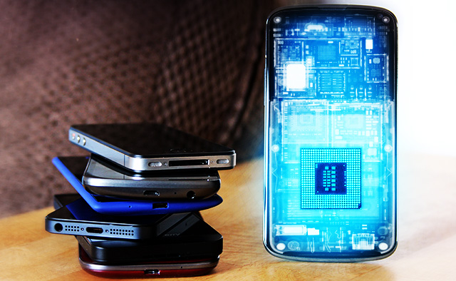
As chip manufacturing processes have improved, it's now possible to cram more and more of these previously separate components into a single chip. This not only reduces system complexity, cost, and power consumption, but it also saves space, making it possible to fit a high-end computer from yesteryear into a smartphone that can fit in your pocket. It's these technological advancements that have given rise to the system-on-a-chip (SoC), one monolithic chip that's home to all of the major components that make these devices tick.
The fact that every one of these chips includes what is essentially an entire computer can make keeping track of an individual chip's features and performance quite time-consuming. To help you keep things straight, we've assembled this handy guide that will walk you through the basics of how an SoC is put together. It will also serve as a guide to most of the current (and future, where applicable) chips available from the big players making SoCs today: Apple, Qualcomm, Samsung, Nvidia, Texas Instruments, Intel, and AMD. There's simply too much to talk about to fit everything into one article of reasonable length, but if you've been wondering what makes a Snapdragon different from a Tegra, here's a start.
Putting a chip together
There's no discussion of smartphone and tablet chips that can happen without a discussion of ARM Holdings, a British company with a long history of involvement in embedded systems. ARM's processors (and the instruction set that they use, also called ARM) are designed to consume very small amounts of power, much less than the Intel or AMD CPUs you might find at the heart of a standard computer. This is one of the reasons why you see ARM chips at the heart of so many phones and tablets today. To better understand how ARM operates (and to explain why so many companies use ARM's CPU designs and instruction sets), we first must talk a bit about Intel.
Intel handles just about everything about its desktop and laptop CPUs in-house: Intel owns the x86 instruction set its processors use, Intel designs its own CPUs and the vast majority of its own GPUs, Intel manufactures its own chips in its own semiconductor fabrication plants (fabs), and Intel handles the sale of its CPUs to both hardware manufacturers and end users. Intel can do all of this because of its sheer size, but it's one of the only companies able to work this way. Even in AMD's heyday, the company was still licensing the x86 instruction set from Intel. More recently, AMD sold off its own fabs—the company now directly handles only the design and sale of its processors, rather than handling everything from start to finish.
ARM's operation is more democratized by design. Rather than making and selling any of its own chips, ARM creates and licenses its own processor designs for other companies to use in their chips—this is where we get things like the Cortex-A9 and the Cortex-A15 that sometimes pop up in Ars phone and tablet reviews. Nvidia's Tegra 3 and 4, Samsung's Exynos 4 and 5, and Apple's A5 processors are all examples of SoCs that use ARM's CPU cores. ARM also licenses its instruction set for third parties to use in their own custom CPU designs. This allows companies to put together CPUs that will run the same code as ARM's Cortex designs but have different performance and power consumption characteristics. Both Apple and Qualcomm (with their A6 and Snapdragon S4 chips, respectively) have made their own custom designs that exceed Cortex-A9's performance but generally use less power than Cortex-A15.
The situation is similar on the graphics side. ARM offers its own "Mali" series GPUs that can be licensed the same way its CPU cores are licensed, or companies can make their own GPUs (Nvidia and Qualcomm both take the latter route). There are also some companies that specialize in creating graphics architectures. Imagination Technologies is probably the biggest player in this space, and it licenses its mobile GPU architectures to the likes of Intel, Apple, and Samsung, among others.
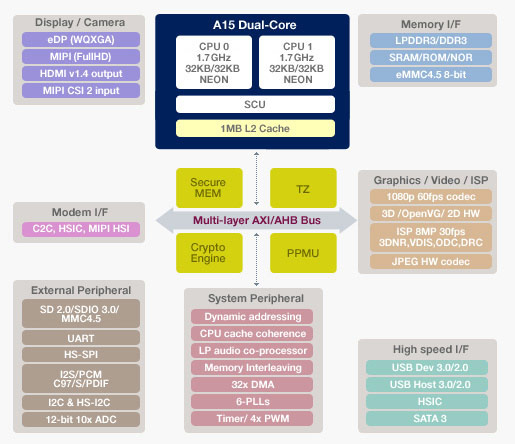
Chip designers take these CPU and GPU bits and marry them to other necessary components—a memory interface is necessary, and specialized blocks for things like encoding and decoding video and processing images from a camera are also frequent additions. The result is a single, monolithic chip called a "system on a chip" (SoC) because of its more-or-less self-contained nature.

There are two things that sometimes don't get integrated into the SoC itself. The first is RAM, which is sometimes a separate chip but is often stacked on top of the main SoC to save space (a method called "package-on-package" or PoP for short). A separate chip is also sometimes used to handle wireless connectivity. However, in smartphones especially, the cellular modem is also incorporated into the SoC itself.
While these different ARM SoCs all run the same basic code, there's a lot of variety between chips from different manufacturers. To make things a bit easier to digest, we'll go through all of the major ARM licensees and discuss their respective chip designs, those chips' performance levels, and products that each chip has shown up in. We'll also talk a bit about each chipmaker's plans for the future, to the extent that we know about them, and about the non-ARM SoCs that are slowly making their way into shipping products. Note that this is not intended to be a comprehensive look at all ARM licensees, but rather a thorough primer on the major players in today's and tomorrow's phones and tablets.
Nailing ICs Together
Tutorial #71
George A. Riley
February 2007
George A. Riley
February 2007
INTRODUCTION
A promising technique for high-density 3-D stacked ICs (SiC) is to directly interconnect stacked die with copper “nails” instead of the wire bonds.
First-generation stacked die in chip-scale packages depend upon multi-level wire bonding for interconnections. (Figure 1) While IC packaging density is increased, signal speed is limited by the inductance and capacitance of the long wire bonds.
Also, wire bonds require relatively large pads, and cannot provide minimum length direct chip to chip functional block connections within the die. Most present applications are for stacked memory die with peripheral bonding pads.

Figure 1. Stacked die with wire bond interconnections in a chip-scale package.
(ChipPAC photo)
(ChipPAC photo)
Continuing research by IMEC has developed through-wafer direct die-to-die copper area-array interconnections. [1] Protruding ends of through-wafer copper vias (“nails”) placed anywhere on the die are directly connected to an adjacent die by thermo-compression bonding.
Advantages of nailed stacked die include:
- Higher speed
- Lower power consumption
- Smaller die size
- Shortest path length
- Functional block interconnections
- Highest interconnect density
- Stacking different devices and technologies.
Figure 2 diagrams copper nail connection of two thinned die to a third die. [2] The 5 micron diameter vias allow a connection density of up to 10,000 vertical connections per square millimeter of surface area. The die could be logic, memory, detectors, and MEMS devices — all be connected in one stack.

Figure 2. Interconnection diagram. (Courtesy IMEC)
In Figure 2, all three of the ICs (gray areas) show several layers of copper metallization (red) applied in standard back-end-of-line (BEOL) processing. The BEOL areas on the surface of each die are shown as magenta.
The copper nails are the vertical red lines linking to the BEOL metallization of each thinned die. An oxide layer (light-blue) insulates the nail from the innards of the die. The die are bonded into a stack by adhesive layers (green).
PROCESS FLOW
After the wafer completes FEOL processing in the wafer foundry, sprayed photoresist is patterned for the interconnection vias. [3] The 5 micron diameter high aspect ratio vias are etched 25 microns into the silicon from the top side. [4] The vias are copper-filled during the first BEOL metallization step. The wafers then continue to normal BEOL processing.
Figures 3a through 3f illustrate the key thinning, etching, and bonding steps after leaving the wafer line for post-BEOL processing of the filled vias. [5]

Figure 3a. The first post-processing step after leaving wafer fabrication is attaching a carrier wafer so that the device wafer can be handled and thinned. Controlling the glue layer thickness and planarity are critical to minimizing total thickness variation across the wafer. The glue must hold the wafer firmly to the carrier, but be easily removable without residues. [6]

Figure 3b. After attaching the carrier, the wafer is first thinned by grinding to remove about 675μm of silicon. This brings the lower surface close to the bottom of the vias. Grinding must be carefully controlled to maintain planarity and not affect chip performance.

Figure 3c. Thinning is completed by chemical-mechanical planarization (CMP) to planarize the bottom of the wafer and to expose and planarize the copper nails.

Figure 3d. An etching step removes silicon, lowering the bottom surface about one micron and exposing that length of the nails. The following SEM photo shows a single copper nail protruding above the wafer surface after silicon etching: [2]


Figure 3e. Sawing the wafer and carrier provides individual single die. For stacking, a die is aligned and connected by simultaneous thermocompression bonding of all its copper nails to the copper landing pads of the next die or wafer. The best reported results were obtained with a citric acid pre-bond surface treatment and a nitrogen blanket to limit oxidation during bonding. [7]

Figure 3f. The final step is to remove the carrier. Another die can then be nailed to previously-formed landing pads on top of this one.
RESULTS
Testing of nailed assemblies showed normal die shear strengths and connection resistances. Daisy-chain test assemblies showed up to 10,000 good vias. Figure 4 is a portion of one daisy-chain assembly after the die silicon was completely removed, revealing the vertical shafts of the copper nails, and the rectangular copper daisy-chain connecting pads, which had once been on the surface of the die. [2]

Figure 4. Portion of a daisy-chain structure after removing the silicon to reveal the vertical copper nails and connecting pads.
CONCLUSIONS
IMEC has clearly demonstrated and documented the feasibility of copper nails for direct chip stacking. Several challenges to commercialization are being addressed. Aggressive thinning of die is limited by possible internal damage. Thermal considerations become critical as stack power density increases, especially if heterogeneous die differ in their thermal expansion coefficients.
Reliability and yield remain to be established, and they will largely determine costs and commercial applications. For volume production, the equipment, skills, process flow and costs must ultimately be within the reach of commercial foundries.
Still, our industry mantra remains “Smaller, faster, lower cost” – and IMEC’s “nailed die” have already achieved two of the three.
REFERENCES
1. P. De Moor, W. Ruythooren, P. Sousan, B. Swinnen, C. Van Der Hoof, E. Beyne, “Recent Advances in 3D Integrations at IMEC,” MRS Fall Meeting, November 27 – December 1 2006, Boston.
2. W. Ruythooren, S. Stoukatch, K. Lambrinou, P. De Moor, B. Swinnen, “Direct Cu-Cu Thermo-Compression Bonding for 3-D Stacked IC Integration,” IMAPS 2006, October 8 – 12, San Diego.
3. N. Pham, M. Vanden Bulche, P. De Moor, “Spray Coating of Photo Resist for Realizing Through-Wafer Interconnects,” EPTC 2006, December 6 – 8, Singapore.
4. D. Tezcan, K. De Munck, N. Pham, O. Luhn, A. Aarts, P. De Moor, K. Baert, C. Van Hoof, “Development of Vertical and Tapered Via Etch for 3D Through Wafer Interconnect Technology, ” EPTC 2006, December 6 – 8, Singapore.
5. K. De Munck, J. Vaes, L. Bogaerts, P. De Moor, C. Van Hoof, B. Swinnen, “Grinding and Mixed Silicon Copper CMP of Stacked Patterned Wafers for 3D Integration” MRS Fall Meeting, November 27 – December 1 2006, Boston.
6. K. De Munck, L. Bogaerts, D. Tezcan, P. De Moor, B. Swinnen, K. Baert, C. Van Hoof, “Wafer Level Temporary Bonding/Debonding for Thin Wafer Handling Applications,” IMAPS International Conference and Exhibition on Device Packaging, March 2006, Scottsdale.
7. B. Swinnen, W. Ruythooren, P. De Moor, L. Bogaerts, L. Carbondell, K. De Munck, B. Eyckens, S. Stoukatch, D. Tezcan, Z. Tökei, J. Vaes, J. Van Aelst, E. Beyne, “3-D integration by Cu-Cu thermo-compression bonding of extremely thinned bulk-Si die containing 10 μm pitch through-silicon vias,” IEDM 2006, December 11 – 13 2006, San Francisco
FOR MORE INFORMATION
The primary source is the referenced IMEC papers, which contain far more information than cited here. For further details, contact IMEC
No comments:
Post a Comment